

The Compute Crunch
A look at the chips, machines and bottlenecks that will decide whether AI delivers on its promise

Almost everything I read on LinkedIn is about two things: software, and services. Funding rounds, law firm innovation projects, AI-native law firms.
What we don’t discuss is that almost every aspect of these businesses now interacts with the physical infrastructure of AI: the data centres, the chips, the machines that make the chips, the companies that make the machines, and so on down the supply chain.
Behind every prompt, Word plugin and tabular review sits an incredibly complex and increasingly strained global supply chain, perhaps the most complex in human history. It depends on a handful of companies, most of which you have never heard of, operating in a handful of countries, several of which sit at the centre of intensifying geopolitical rivalry.
On a couple of long train journeys recently, and after listening to this excellent podcast, I found myself going down the rabbit hole. And the more I did, the more I realised that:
The hardware and infrastructure side is going to shape what happens next far more than any legal tech company or law firm.
Understanding this now can help you see around corners, make better decisions about where to invest, and how to plan for the next few years.
It starts with a prompt
Let’s consider what happens when a lawyer prompts an AI tool to review a contract.
In the two seconds before the response appears, the query hits an API that calls a frontier model running on GPUs in a data centre consuming megawatts of electricity and millions of gallons of cooling water. Those GPUs were fabricated by a single company in Taiwan, on silicon wafers, using patterns printed by a machine that can only be made by one company, operating out of a small town in the Netherlands. That machine relies on mirrors made by a company in Germany that are so precise that if one were scaled to the size of the country, the tallest bump on its surface could not exceed one centimetre.
And every one of those steps has a bottleneck.
Bottleneck 1: The Most Complicated Machine in the World
In Veldhoven, a quiet town near Eindhoven in the south of the Netherlands, is a company called ASML. It barely comes up in discussions about AI. I confess I had never heard of it. But with a market cap of $527 billion, it is now the largest company in Europe, and there is a case for saying it might be the most important company in the world right now. It has no meaningful competitor.
What does ASML do? It makes a machine called the Extreme Ultraviolet lithography system, known as an EUV, a tool for printing the microscopic circuit patterns on silicon wafers that create every leading-edge chip on the planet. Without these machines, not a single advanced Nvidia GPU, Google TPU, Apple processor, or AMD chip gets made. Your AI-powered contract review, your due diligence assistant, your research tool: none of them exist without this machine.
To understand why ASML is the single biggest bottleneck in the AI supply chain, you need to understand what its machine actually does.

The features on a modern chip are a few nanometres wide. To print patterns that small, you need light with an extremely short wavelength, 13.5 nanometres, in the extreme ultraviolet range. This light does not exist in any naturally useful form, so it has to be manufactured. ASML’s machine does this by dropping tiny droplets of molten tin into a vacuum chamber. A laser hits each droplet three times in rapid succession: the first pulse shapes it, the second flattens it into the ideal geometry, the third blasts it at extreme power, exciting the tin atoms until they emit photons at exactly 13.5 nanometres. This happens 50,000 times per second.
EUV light is absorbed by virtually everything, including glass, so conventional lenses are useless. Instead, the light bounces off a series of multilayer mirrors manufactured by Carl Zeiss in Germany. You might recognise that name from your camera lens. Each mirror is built from alternating layers of molybdenum and silicon, deposited atom by atom. The precision is staggering: if one of these mirrors were scaled to the size of Germany, the tallest bump on its surface could not exceed one centimetre. Zeiss produces these optics in quantities of hundreds per year. The process is closer to artisanal craftsmanship than to mass production.
This has been described as the most complicated machine in the world. The whole tool weighs over 150 tonnes, fills the space of a double-decker bus, ships in 40 freight containers, and takes months to install.
Each machine costs $300 to $400 million. ASML currently produces about 70 per year, growing to perhaps just over 100 by the end of the decade.
It will not be enough.
Roughly 3.5 EUV tools are needed per gigawatt of AI compute. Those tools cost about $1.2 billion. The data centre they enable costs $50 billion. The AI revenue generated on top could be $100 billion or more. An astonishing economic pyramid resting on a narrow physical base.
The obvious question is: why not just build more of them? One, because it’s really really hard; and two, because the companies who make these things haven’t yet been convinced to ramp up more aggressively.
An EUV machine is not a product that can be scaled like software or even like a conventional manufacturing line. It is an assembly of roughly 100,000 components sourced from hundreds of suppliers across multiple countries, many of whom are themselves the only company in the world that makes their particular part. The Zeiss mirrors alone take months to produce, require atom-by-atom deposition of alternating layers, and are made in quantities of hundreds per year by a workforce of highly specialised technicians. You cannot train those people quickly. You cannot build a second Zeiss mirror line the way you might open a second factory for car parts. The knowledge is embodied in the people and the processes, not in a blueprint you can hand to a contractor.
The same is true of the Cymer laser sources (the systems that generate the tin-droplet EUV light), and other components in the machine, each of which has its own supply chain. Each one has its own multi-year production constraints, its own specialised workforce, and its own supplier dependencies. Scaling further would require simultaneous expansion across the entire web of suppliers, many of whom see no reason to invest aggressively because they do not share the AI industry’s demand forecasts.
There is also a more fundamental mismatch at the heart of the AI supply chain. The companies at the top of the stack, the AI labs and hyperscalers, are investing at a pace that implies transformative AI is imminent. The companies at the bottom, the ones who would need to expand to meet that demand, seem to be a bit more sceptical. They have seen technology hype cycles before. They are not going to bet their businesses on demand projections from Silicon Valley. The companies at the top see a revolution. The companies at the bottom see a cycle.
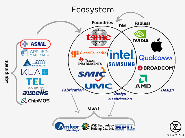
Bottleneck 2: The Foundry
ASML makes the tool. But the company that uses the tool (and others) to manufacture the actual chips is Taiwan Semiconductor Manufacturing Company, or TSMC, headquartered in Hsinchu, Taiwan. TSMC is the world’s largest and most advanced chip foundry. It fabricates chips for virtually every major technology company: Nvidia, Apple, AMD, Google, Amazon, Qualcomm, Broadcom, and many others.
TSMC’s manufacturing processes, currently at the 3-nanometre node with 2-nanometre in development, produce the highest yields and best performance in the industry. Samsung has struggled with yields on its most advanced nodes. Intel is aggressively trying to rebuild its foundry business, but it is years behind TSMC in high-volume production. For the foreseeable future, leading-edge AI chips are TSMC chips.
TSMC does not have infinite capacity. It needs to decide what to prioritise. The race for capacity at TSMC has already produced winners and losers. Nvidia saw what was coming and committed to non-cancellable orders years in advance. By 2027, Nvidia is projected to control over 70% of TSMC’s 3nm wafer capacity. Google and Amazon, which design their own AI chips, moved more cautiously and found themselves capacity-constrained when their AI revenue began to surge.
(Side note: Anthropic was similarly conservative about long-term compute contracts from the cloud vendors, wanting to avoid financial risk. OpenAI signed aggressively with every provider it could find. Now OpenAI has more compute at better prices, while Anthropic scrambles to acquire capacity from less established providers at higher cost. This gives OpenAI a huge advantage and I’m not sure people are talking enough about this.)
The lesson at every level of the stack is the same: caution was punished.
TSMC itself prefers to allocate capacity to stable, predictable businesses like CPUs rather than the volatile AI chip market, a conservatism that has further advantaged Nvidia, whose massive pre-commitments made it look like the safe bet. And because chip supply is constrained, what prices a GPU is not the alternative you could buy, but the value you can extract from it. Today’s AI models are dramatically more capable than the models that ran on H100s at launch. Each GPU produces more tokens of a higher-quality model, serving a larger market. Because of the supply constraints, older hardware is actually worth more today than it was a couple of years back, not less.
Bottleneck 3: Memory
An AI chip is two things working together: a processor that does the mathematics, and memory that holds the data the processor needs. Without fast, abundant memory right next to the processor, the most powerful chip in the world doesn’t do very much.
The memory used in AI chips is called high-bandwidth memory, or HBM: stacks of chips layered on top of each other and connected with thousands of tiny wires for maximum data throughput. A single gigawatt of Nvidia’s upcoming Rubin chips requires approximately 170,000 wafers of memory chips.
Two companies dominate HBM production. SK Hynix, a South Korean company, is the market leader and Nvidia’s primary memory supplier. Samsung Electronics is the other major player, though it has trailed SK Hynix in the latest HBM generations. Memory is manufactured in its own fabs, using its own set of EUV lithography, which means it competes for the same scarce ASML machine time as the logic chips it sits beside. Memory vendors are aggressively raising prices, doubling and tripling in some cases, and signing long-term contracts. Nvidia has negotiated three-year deals with memory suppliers to secure allocation.
The same pattern repeats: every component in the AI supply chain ultimately queues behind the same handful of machines in Veldhoven.
Bottleneck 4: Power, Water, and the Physical World
The five largest hyperscalers (Amazon, Google, Meta, Oracle, and Microsoft) collectively plan to spend up to $700 billion in capital expenditure this year, with roughly three quarters going to AI infrastructure. Amazon alone expects to spend $200 billion, a number so large it will likely push the company’s free cash flow negative for the year. Google’s Larry Page has been quoted saying he would rather go bankrupt than lose this race.
To put this in perspective, the entire GDP of Sweden is about $600 billion. The combined AI infrastructure spend of five American technology companies in a single year now exceeds that.
These are not abstract financial commitments in a spreadsheet. They are construction projects. A single hyperscale AI data centre can consume as much electricity as two million US households. Meta is building a facility in Louisiana that could eventually scale to five gigawatts, roughly the output of five nuclear power plants. Microsoft has an $80 billion backlog of Azure orders it cannot fulfil because the power infrastructure does not yet exist.
Data centres are going up fast. Amazon has brought facilities online in as little as eight months. Google has acquired an energy company outright, is putting deposits on gas turbines for 2028 and 2029, and is buying large tracts of powered land. But the physical consequences are becoming harder to ignore, and for lawyers, regulators, and their clients, they are becoming impossible to avoid.
AI data centres are extraordinarily thirsty. Google’s facilities consumed 5.6 billion gallons of water in 2023, a 24% increase over the previous year. In The Dalles, Oregon, Google’s three data centres use more than a quarter of the city’s water supply. In Chile and Uruguay, protests have erupted over planned facilities that would draw from the same reservoirs that supply drinking water. By 2028, data centres across the US could collectively consume as much water as 18.5 million households.
The electricity numbers are equally stark. In 2023, AI and data centres accounted for roughly 4% of US electricity consumption. That share is expected to triple by 2028. Ireland already dedicates over 20% of its national electricity to data centres. In Virginia, the figure is 26%. Microsoft pledged to go carbon negative by 2030. Its total emissions in 2024 were 30% higher than in 2020, driven by AI infrastructure expansion.
Communities are pushing back. Data centres in Northern Virginia, the densest concentration in the world with roughly 300 facilities, are expanding into farmland and generating noise, diesel exhaust from backup generators, and rising utility bills for residents. New York is considering a three-year moratorium on large new projects while it studies their environmental and energy impacts.
Environmental, planning, and regulatory questions are accumulating faster than the legal and policy frameworks needed to answer them. Every one of those questions is potential work. And every one of them is a potential constraint on the buildout that the AI industry is counting on.
The consensus among supply chain analysts is that power in the United States will not be the binding constraint on AI scaling in the near term. Data centres are simpler to build than semiconductor fabs, the money is available, and the engineering is well understood. But adding tens of gigawatts of capacity in a single year places enormous strain on electrical grids, turbine suppliers, transformer manufacturers, and permitting processes. As chip supply eventually catches up with demand, power could resurface as the bottleneck in the late 2020s.
There are more radical ideas on the table. Elon Musk has publicly discussed deploying up to 100 gigawatts of compute in space per year, using solar power in orbit where sunlight is continuous and land constraints vanish. Solar energy in space is roughly seven times more efficient than on the ground, and cooling in the vacuum of space is well understood for satellites. But the concept runs directly into the bottleneck described throughout this article. Even if you could generate unlimited power in orbit, you still need chips to put there, and those chips all have to pass through ASML’s EUV machines and TSMC’s fabrication lines. The power problem might be solved in space. The semiconductor supply chain is earthbound.
Bottleneck 5: Atoms
Behind the supply chain constraints lies a deeper, more fundamental one: the laws of physics.
For sixty years, the semiconductor industry has been governed by Moore’s Law, the observation that the number of transistors on a chip doubles roughly every two years. This was enabled by making transistors smaller with each generation: from micrometres in the 1970s, to hundreds of nanometres in the 1990s, to single-digit nanometres today. An AI chip like Nvidia’s H100 contains roughly 80 billion transistors, each one a few nanometres across, about the width of five silicon atoms.
Jensen Huang, Nvidia’s CEO, has stated it plainly: “We can keep shrinking transistors, but we can’t shrink atoms.” A silicon atom is about 0.2 nanometres wide. At the 2-nanometre node, which TSMC is now entering production on, a transistor is roughly ten atoms across. At these scales, quantum effects become significant: electrons tunnel through barriers they should not be able to pass, causing current to leak. Leaking current means wasted energy and heat. A related rule called Dennard scaling, which promised that smaller transistors would use less power, broke down around 2005. The pace of improvement has slowed from roughly 10x every five years to about 2x every five years.
The industry is buying time through several strategies. New transistor designs like “gate-all-around transistors”, which wrap the gate around the channel on all four sides, give better control over current at small scales. 3D stacking builds up rather than shrinking down, layering chips vertically. Chiplet architectures place multiple smaller dies side by side rather than trying to make one enormous chip.
There is also a more radical possibility. Neuromorphic computing attempts to build chips that work more like the human brain, which runs on roughly 20 watts (about the same as a couple of LED bulbs) while performing cognitive tasks that still exceed AI in many domains. Intel’s Loihi 3 chip, released in January 2026, packs 8 million artificial neurons and operates at a peak of approximately 1.2 watts, compared to 300 or more watts for a GPU doing equivalent real-time inference. IBM’s NorthPole chip achieves up to 25 times the energy efficiency of an H100 for image recognition.
The catch is that neuromorphic chips cannot yet run large language models. They excel at sensory processing and real-time pattern recognition, not the dense matrix multiplication that powers a conversation with Claude. But there is a plausible future in which neuromorphic architectures handle perception and real-time processing while GPUs handle reasoning and language, dramatically reducing the total compute demand on the constrained supply chain. Some researchers, including Yann LeCun (formerly the brains behind Meta’s AI strategy), believe entirely different AI model architectures known as “World Models” focused on understanding the world and fundamental concepts rather than focusing on language may eventually sidestep the GPU bottleneck altogether, at least for robotics use cases.
None of this will change the fundamental picture within the next five years. The industry is locked into the GPU-and-transformer paradigm. But the atomic wall is real, and the long-term future of AI may depend on architectures that work with the physics rather than fighting against it.
Bottleneck 6: Geography and Geopolitics
The overwhelming majority of advanced chip manufacturing capacity is located on an island of 23 million people in the western Pacific. Taiwan’s status, and the security of TSMC’s fabs, is one of the defining strategic questions of the coming decades.
If TSMC’s Taiwan fabs went offline, the consequences would be immediate. Every Nvidia GPU, every Google TPU, every Apple processor in current production depends on them. The chips already deployed in data centres would become irreplaceable and astronomically valuable. AI progress would effectively freeze at whatever capability existed at the time of disruption.
The export control regime coordinated between the US, Netherlands, and Japan uses ASML’s EUV monopoly as the centrepiece of a deterrence strategy: China cannot manufacture advanced chips without EUV tools, and it cannot acquire them. Running a seized TSMC fab without ongoing support from ASML, Applied Materials, Lam Research, and other Western and Japanese suppliers would be effectively impossible. The equipment would degrade and stop producing within months.
TSMC is building fabs in Arizona, Japan, and Germany to diversify. But these are smaller and behind the cutting edge. Meaningful geographic diversification of advanced manufacturing is an early-2030s proposition at best. Until then, the physical infrastructure powering every frontier AI model is concentrated in one of the most geopolitically sensitive locations on Earth.
What this means for legal
I’ll say at the start that there are too many variables right now for anyone to know for sure how all this plays out. But if compute does indeed become more constrained and expensive, there are some potential consequences that firms and vendors should plan for.
Costs are probably going up, not down
All the legal AI vendors build on frontier model APIs and are exposed to the underlying cost of compute. As the labs raise prices to manage demand within increasingly constrained capacity, those costs flow downstream.
Vendors on flat per-seat pricing models (most or all of them right now, I believe) will face pressure to shift toward consumption-based pricing. Firms should obviously budget for legal AI costs to rise when their current fixed term deals (most of them 2-3 years) come to an end.
On a consumption-based model, this also raises the question of whether tokens or compute get billed through to the client like photocopying disbursements.
Context engineering and model routing become critical
A practical consequence of the compute crunch is that how you use the model matters almost as much as which model you use.
Context engineering, the discipline of structuring what you send to the model so that it produces the best possible output with the fewest possible tokens, is becoming a genuine competitive advantage. A well-engineered prompt that gives the model exactly the right context in a compact form gets a better answer at lower cost than a lazy prompt that dumps in everything and hopes for the best. For legal technology vendors, this is an engineering challenge with direct commercial implications. For law firms, it is a skill that might separate effective AI users from expensive ones.
Model routing is the other side of the same coin. Vendors will send simple queries to cheaper, smaller models and reserve frontier models for complex work. This is a rational response to scarcity and cost pressure. But it has implications for quality. A firm may believe it is paying for a frontier model but find that routine queries are being handled by a less capable one. In legal, where a “routine” question can have non-obvious complexity, the distinction matters.
Firms evaluating AI vendors should ask explicitly which models are used for which tasks, whether routing is transparent, and what guarantees exist that high-stakes queries receive frontier-grade processing.
Both of these trends point in the same direction: the era of treating AI as a magic box you throw text into is ending. The firms and vendors that treat compute as a scarce resource to be used skillfully will probably outperform those that treat it as an unlimited commodity.
The human vs AI question continues to be asked
Rising compute costs do not just affect the technology. They affect the fundamental business case for using AI in the first place.
Like it or not, the promise of legal AI has largely rested on the proposition that AI can do certain tasks faster, better and/or cheaper than a human. But “cheaper” depends on the cost of compute. If model costs rise and the tasks that benefit most from AI (complex, multi-step, high-context work) are also the most token-intensive, the calculus might shift. For some workflows, the answer to “should we use AI or a human?” may move back toward the human, at least until the supply chain catches up.
This does not mean AI becomes uneconomic across the board. For the right tasks like high volume doc review, the efficiency gains are large enough to absorb meaningful cost increases. But for bespoke, judgment-heavy work where the AI needs extensive context and multiple reasoning passes, the cost advantage may narrow.
Conclusion
AI is going to transform the legal industry. I don’t think anyone seriously debates that at this point. The models are genuinely capable, improving fast, and rewarding early adoption.
But the physical infrastructure behind them (the silicon, the lithography, the fabs, the memory, the mirrors, the tin droplets, the power) is subject to constraints that no amount of venture capital or algorithmic innovation can immediately overcome, and that has some significant consequences. The most important company in this story is not the one whose name you see on the chatbot interface. It is a company in a small Dutch town, building 70 machines a year, each one a minor miracle of physics and precision engineering, each one indispensable to the future of artificial intelligence.
The next time your AI tool takes two seconds to respond, consider what made those two seconds possible, and what that might mean for your company and its business model in the coming years.
This article draws on reporting and analysis from SemiAnalysis, Dylan Patel’s conversation with Dwarkesh Patel (March 2026), ASML corporate disclosures, Morgan Stanley and Bank of America research, public semiconductor industry data, and Intel, IBM, and Meta research publications.